
One to five layer graphene — grown and precision-stacked — engineered into memory, quantum and terahertz devices.
We work in the regime where graphene stops behaving like a bulk material and starts behaving like a designable electronic system — one to five atomic layers, with stacking order as a design variable.
Wafer-scale monolayer and few-layer films grown by chemical vapour deposition, transferred onto device substrates.
Proprietary layer ordering that unlocks correlated states and superconducting behaviour.
Graphene stacked with dielectrics and 2D partners to engineer bandgap, mobility and coupling.
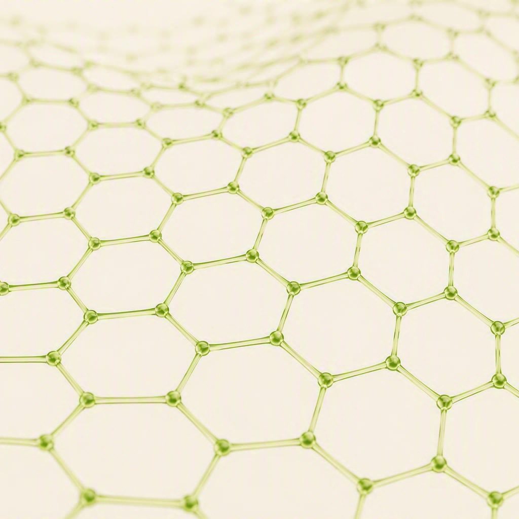 LATTICE_001 — HONEYCOMB
Non-volatile graphene memory targeting high density, low switching energy and strong retention.
Graphene-based Josephson elements for gate-tunable qubits and quantum computing research hardware.
The device stack →Terahertz detectors, modulators and emitters exploiting graphene's ultrafast carrier response.
High-sensitivity sensing and low-resistance interconnect layers for advanced packaging.
Quantum processors today are built from fixed aluminium junctions. Graphene makes the junction itself tunable — turning a fabricated constant into a control knob.
Graphene weak link between superconducting electrodes carries a supercurrent.
Hexagonal boron nitride stacking preserves mobility and interface quality.
An electrostatic gate sets carrier density, and with it the critical current.
Coupled to a microwave resonator for dispersive measurement at millikelvin.
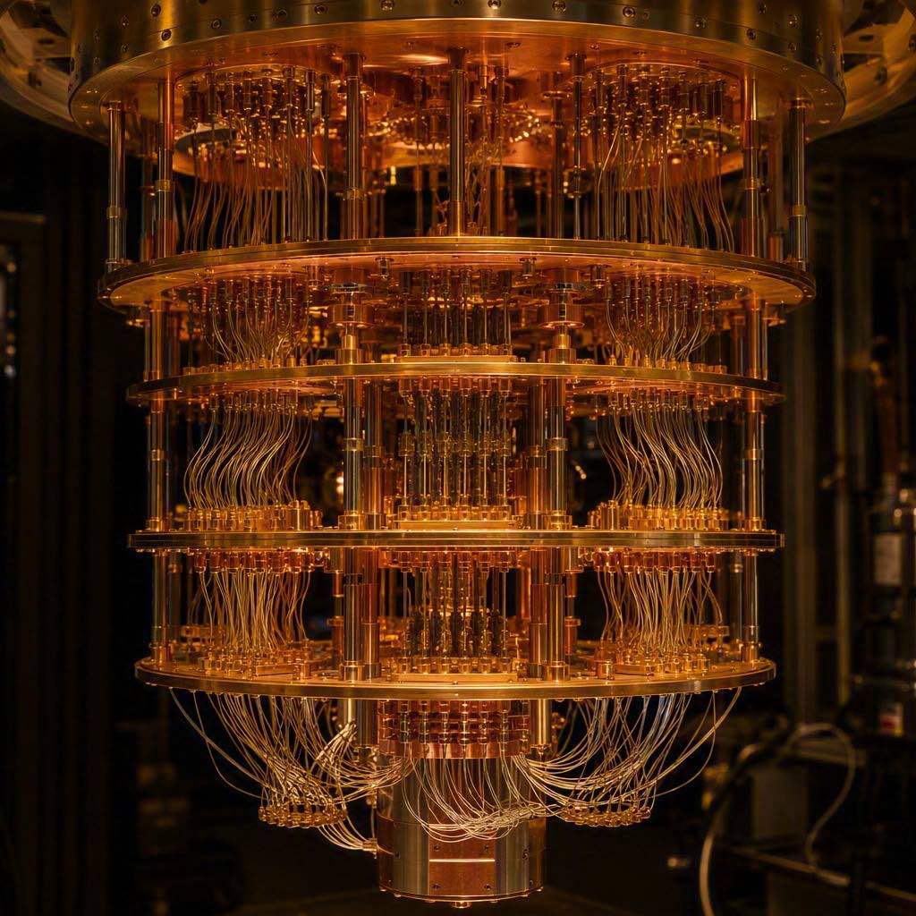 CRYO_001 — MILLIKELVIN STAGE
Electrical gate tuning replaces fixed junction geometry — frequency becomes controllable.
Proprietary layer ordering gives access to correlated and superconducting states by design.
Low intrinsic loss in clean encapsulated stacks supports coherence targets.
Shared fabrication toolchain with our memory and terahertz device lines.
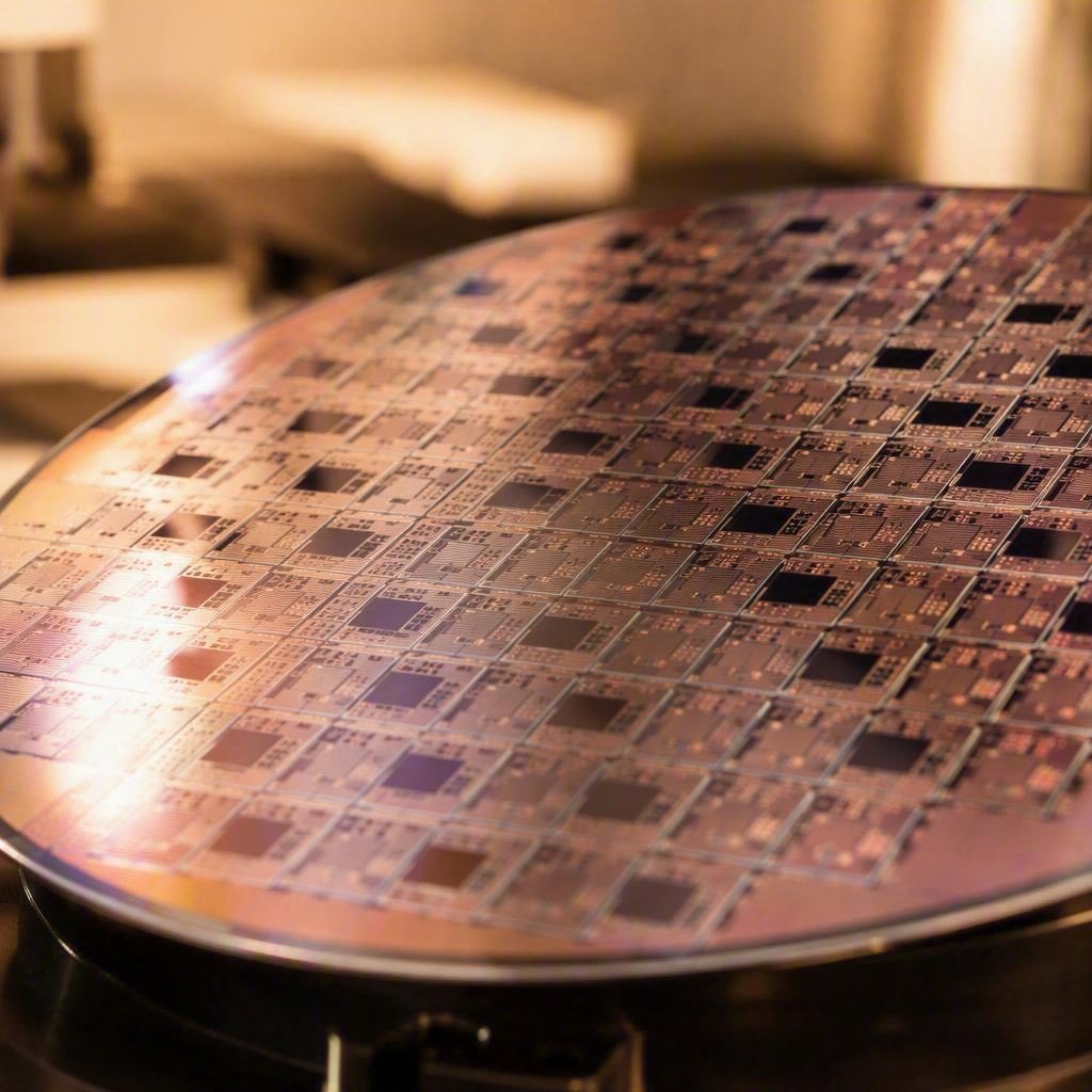 WAFER_012 — POST-TRANSFER
Our Hyderabad centre brings materials characterisation and device fabrication under one roof — so a graphene device stack can be developed, tested and scaled in the same place.
Graphene synthesis, transfer and characterisation.
Device fabrication and cryogenic measurement.
Product testing to industrial and safety standards.
Partnerships with Indian institutes and industry.
Pilot lines sequenced with Soma Technologies materials.